

Atomic-Scale Integration: Analyzing the Advanced Materials for Electronic Market Share
The global electronics manufacturing and telecommunications landscape of early 2026 is operating under a mandate for extreme material safety and signal precision. Central to this transition is the development of robust, high-frequency dielectrics and low-k materials that minimize signal interference in 5G and early-stage 6G devices. As the "Internet of Things" (IoT) connects billions of new sensors, the materials used to package and protect these components must offer superior moisture resistance and thermal dissipation. Unlike legacy materials, modern advanced electronics materials are engineered at the molecular level to provide a "zero-drift" performance, ensuring that critical data remains accurate even under the extreme vibrational and thermal stresses found in autonomous automotive systems.
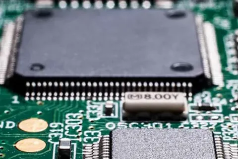
According to a recent report by Market Research Future, the Advanced Materials for Electronic Market is benefiting from the massive expansion of the Semiconductor and Integrated Circuit (IC) segments, which capture over 58% of total material usage. This shift is a primary focus of Advanced Materials for Electronic Market Share analysis, which identifies Silicon Carbide (SiC) as a dominant material type, particularly in the EV sector where it enables higher voltage tolerance and better thermal performance. Key industry leaders such as BASF SE, DuPont, and Samsung SDI are increasingly focusing on Nanotechnology-Enhanced Finishing, where nanomaterials are integrated into photoresists and CMP (Chemical Mechanical Planarization) slurries to achieve the extreme flatness and purity required for next-generation 3nm chip fabrication.
As we look toward the mid-2030s, the focus is shifting toward "Bio-Electronic Convergence" and the expansion of the compostable hardware niche. We are seeing early-stage research into using plant-derived cellulose and biodegradable polymers—a market segment projected to grow at a CAGR of 16.0%—as substrates for low-power consumer devices to address the global electronic waste crisis. Furthermore, the move toward "Photonics-Integrated Packaging"—where light is used alongside electricity for data transmission—is helping the industry overcome the "thermal wall" associated with traditional copper interconnects. By 2035, the market will be a foundational pillar of Aseptic Connectivity, providing the essential, high-purity, and multi-functional materials required to protect and empower global populations in a world of increasingly sophisticated and ecologically conscious digital hardware.